
Atomic layer deposition is a thin film technology that enables very precise nanometer–thick, pinhole–free and totally conformal thin films on any shape and geometry. During the coating process, two or more chemical vapors or gaseous precursors
react sequentially on the substrate surface, producing a solid thin film. ALD can deposit superior quality coatings on wafers, planar objects, porous bulk materials and complex 3D objects with very high aspect ratio (HAR) features.
Typical
characterization techniques for ALD layers:
- Ellipsometry
- Atomic Force Microscopy
- Scanning Electron Microscopy
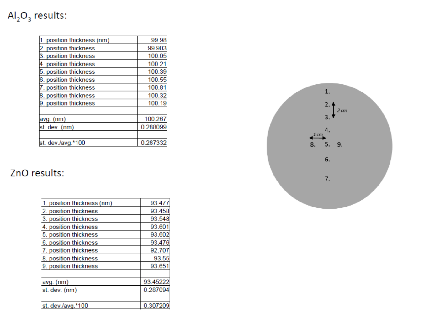
Ellipsometry measurements: Al2O3 on a 200 mm silicon wafer using trimethylaluminum (TMA) and H2O precursors with film thickness 100 nm and variation within the 200 mm wafer 0.28% and ZnO on a 200 mm silicon wafer using diethylzinc (DEZ) and H2O precursors with film thickness 93 nm and variation within the 200 mm wafer 0.3%.