
Our recently developed custom-designed micro-scale photoelectrochemical setup (Figure 1.) allows us to study the photoelectrochemical (PEC) behaviour under illumination with controlled wavelength and intensity. This approach can identify the structural parts of layered transition metal dichalcogenides (TMDCs) and to measure the PEC activity (photovoltammetry, photocurrent transient analysis, and quantum efficiency, Figure 2.) of the exfoliated two-dimensional (2D) flakes using a 10-50 μm droplets in diameter. The deep understanding of the PEC activity of 2D semiconductors as a function of their structural properties is critical for their successful implementation in solar energy conversion.
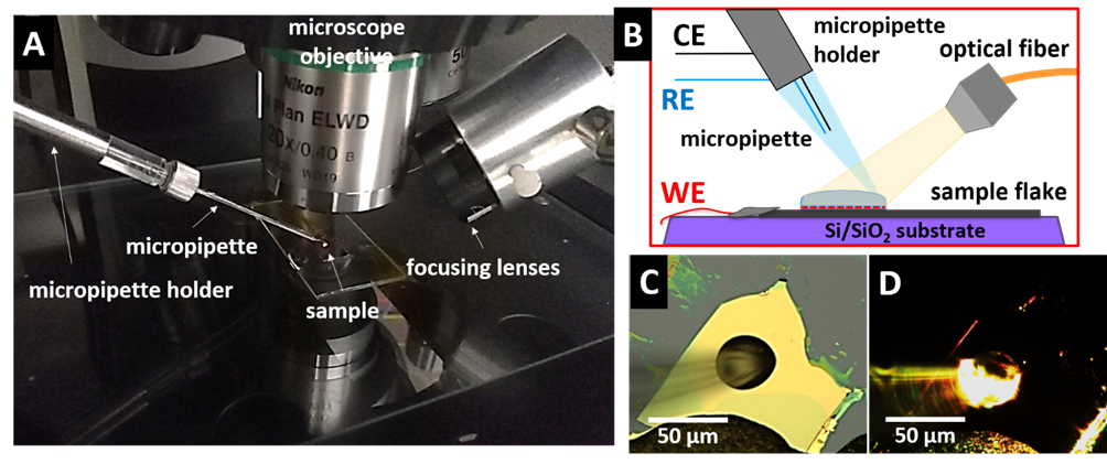
Introduction of the micro-droplet photoelectrochemical system, and microscopic characterization of MoSe2 bulk flakes. A: Photograph of the sample area under the microscope objective. B: Scheme of the photoelectrochemical setup. Optical micrographs of a droplet deposited on the surface of a single crystal bulk MoSe2 flake, without (C) and with (D) white light illumination.
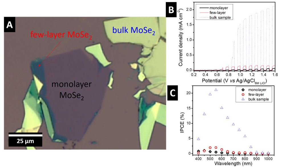
PEC behaviour of layered specimens. A: Optical micrograph of an MoSe2 flakes on SiO2/Si substrate. B: LSVs recorded for the illuminated droplets deposited on mono,- few-layers and bulk flakes, of MoSe2. b) Quantum efficiency curves show different
behaviours between the PEC activity of mono,- few-layers and bulk flakes, of MoSe2.