
A KP Technology APS04 instrument is available to perform contact potential,
surface photovoltage and ambient pressure photoelectron spectroscopy measurements.
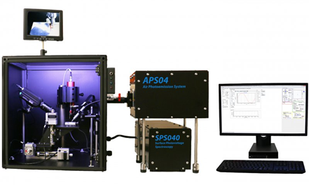
Contact potential difference (CPD) can be measured between the sample and the tip of the Kelvin probe. During these measurements a 2 mm diameter gold alloy-coated tip is vibrated above the sample surface at a constant height (∼1 mm) and amplitude (0.2
mm), with a constant frequency (70 Hz). From these measurements the Fermi-level of the samples can be determined. The instrument is also capable of mapping the sample surface. Illuminating the sample surface with a 150 W quartz halogen lamp (Fiber-Lite
DC950) coupled with a monochromator allows us to perform surface photovoltage (SPV) measurements. The change in the contact potential difference in semiconductor samples can reveal:
• type of majority carriers,
• charge transfer pathways,
• bandgap of the semiconductor
• energy level alignments under illumination
Ambient pressure UV photoelectron spectroscopy (UV−APS) can also be carried out with a variable energy UV light source (3 ̶ 7 eV). When the sample surface is illuminated
the UV light generates an electron cloud from the sample if:
• hΦ ≥ EVB for semiconductors,
• hΦ ≥ Φ, where Φ is the sample work function for metals
Under atmospheric conditions through inelastic scattering between the ejected electrons
and atmospheric secondary ions (N2−, O2−) are formed. These ions can be collected by the Kelvin-probe tip, thus a current is measured. This can be used to determine the work function of metals or the valance band position of semiconductors. Together
these three techniques are used by our group for work function measurement of metals and to determine the band diagram of semiconductor systems. Currently the system resides in a glovebox (MBraun) under controlled atmospheric conditions (O2 and H2O
< 1ppm).
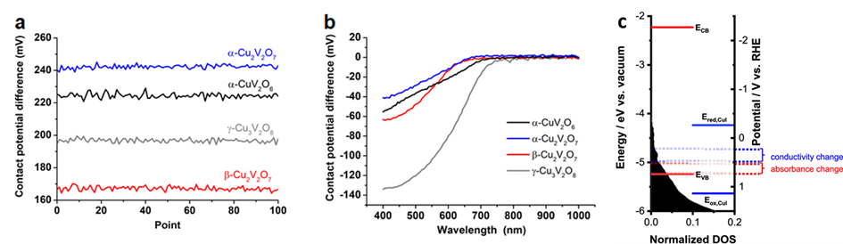
Contact potential difference (a) and surface photovoltage spectra (b) for the different copper vanadate samples. See article [6] for more details. Band diagram of CuI together with the density of states plot (c) determined from CPD and APS measurements.
See article [5] for more details.
[1] A. Kormányos, D. Hursán, C. Janáky - Photoelectrochemical Behavior of PEDOT/Nanocarbon Electrodes:
Fundamentals and Structure–Property Relationships - J. Phys. Chem. C 2018, 122,
13682-13690 DOI:10.1021/acs.jpcc.8b00145
[2]
A. M. Ismail, G. F. Samu, Á. Balog, E. Csapó, C. Janáky - Composition-Dependent
Electrocatalytic Behavior of Au–Sn Bimetallic Nanoparticles in Carbon Dioxide Reduction - ACS Energy Lett. 2019, 4, 48-53 DOI: 10.1021/acsenergylett.8b01996
[3]
A. Ochirkhuyag, I. Y. Tóth, A. Kormányos, C. Janáky, Z. Kónya - Composition-Dependent Optical and Photoelectrochemical
Behavior of Antimony Oxide Iodides - J. Electrochem. Soc. 2019, 166, H3202-H3207 DOI: 10.1149/2.0311905jes
[4]
Á. Balog, C. Janáky - The Effect of Trap States on the Optoelectronic Properties of Nanoporous Nickel Oxide - J. Electrochem. Soc. 2019, 166, H3265-H3270 DOI: 10.1149/2.0361905jes
[5] Á. Balog, G. F. Samu, P. V.
Kamat, C. Janáky - Optoelectronic Properties of CuI Photoelectrodes - J. Phys. Chem. Lett. 2019, 10, 259-264 DOI: 10.1021/acs.jpclett.8b03242
[6] M. K. Hossain, P. Sotelo, H. P. Sarker, M. T. Galante,
A. Kormányos, C. Longo, R. T. Macaluso, M. N. Huda, C. Janáky, K. Rajeshwar - Rapid One-Pot Synthesis and Photoelectrochemical Properties of Copper Vanadates - ACS Appl. Energy Mater. 2019, 2, 2837-2847 DOI: 10.1021/acsaem.9b00179
[7]
P. Sotelo, M. Orr, M. T. Galante, M. K. Hossain, F. Firouzan, C. Longo, A. Kormányos, H. P. Sarker, C. Janáky, M. Huda, K. Rajeshwar, R. Macaluso - Role of Electrons in the Optical and Photoelectrochemical Behavior of Ca(La1–xCex)2S4 (0 ≤ x ≤ 1) - Inorg. Chem. 2019, 58, 4553-4560 DOI: 10.1021/acs.inorgchem.9b00062
[8] A. M. Ismail, E. Csapó, C. Janáky - Correlation between the work function of Au–Ag nanoalloys and their electrocatalytic activity in carbon dioxide reduction -
Electrochimica Acta 2019, 313, 171-178. DOI: 10.1016/j.electacta.2019.05.016
A Specs XPS instrument equiped with an UVS10/35 system is at our disposal to perform UPS measurements under ultrahigh vacuum conditions (XPS main chamber pressure in 10-9 mbar – 10-10 mbar range). By varying the He pressure in the discharge lamp
both He(I) (21.22 eV) and He(II) (40.8 eV) excitation can be used.
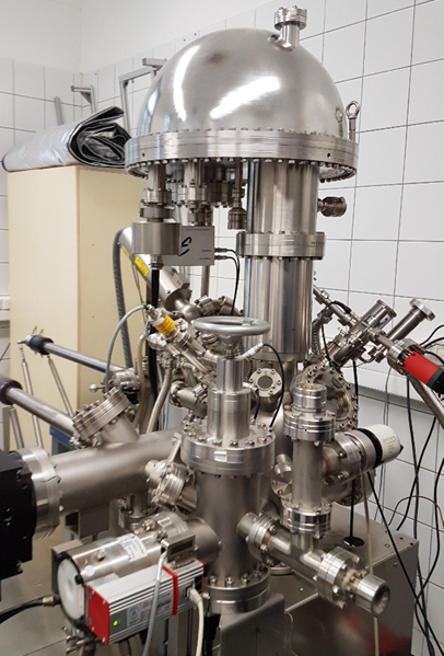
Picture of the SPECS XPS UPS instrument
Determination of the sample Fermi-edge, work function can be performed. In the case of semiconductors the density of states in the valence band can be experimentally determined. In the case of metals the experimental determination of the d-band
structure is also possible.